 MENU
MENU 

EECS 521: Solid State Devices
Instructor: Professor Wei Lu
Coverage
This is a graduate level course aimed to provide students a comprehensive understanding of solid state electronic devices, emphasizing on the challenges facing CMOS scaling and possible solutions. The course covers fundamental advanced topics in MOSFET devices, nanoscale planar and non-planar silicon transistor structures, and some promising research device structures.
Textbook(s)
Fundamentals of Modern VLSI Devices by Yuan Taur and Tak H. Ning
Cambridge University Press, 1st edition (October 13, 1998) ISBN: 0521559596
Schedule
| Lecture 1 Introduction. | (ITRS’s PIDS and ERD chapters, Intro to Nanoscale devices). Free electron model |
| Lecture 2 Electrons in solids. | Density of states, Fermi surfaces, tight-binding model, energy bands, carrier density, (notes) |
| Lecture 3 Energy bands. | Si and GaAs lattice and band structures, valley degeneracy, HH and LH bands (Waser 3, Davies 2) |
| Lecture 4 Scattering and mobility | Envelope function, doping, scattering time approximation, mobility, phonons, screening (Waser 3, Davies 2) |
| Lecture 5 MOS capacitor | Surface potential, inversion, exact charge solutions. C-V, interface charges, intro to MOSFET (Taur 2.3) |
| Lecture 6 MOSFET devices | Drain-current model based on gradual channel approx, I-V characteristics, channel mobility (Taur 3) |
| Lecture 7 MOSFET, beyond long channel model | Subthreshold region, Degradation of the effective mobility, finite inversion layer capacitance, Short-channel effects (DIBL and charge-sharing model) (Taur 1.2, 3.2, 2.4) |
| Lecture 8 High-field effects | Velocity saturation, impact ionization, LDD, band-to-band tunneling, GIDL, dielectric breakdown (Taur 2.4) New devices based on tunneling and impact ionization effects. |
| Lecture 9 Scaling rules and CMOS device design parameters | Scaling rules, threshold voltage design (Taur 4.2) |
| Lecture 10 SOI devices | Non-scaling factors, advantages of thin-body SOI electrostatics (Taur 4.1, 5.4, notes) |
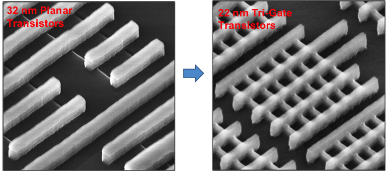
| Lecture 11 Multiple-gate MOSFETs | Thin-body MOSFET carrier transport, double gate devices, GAA devices, parasite resistance ( |
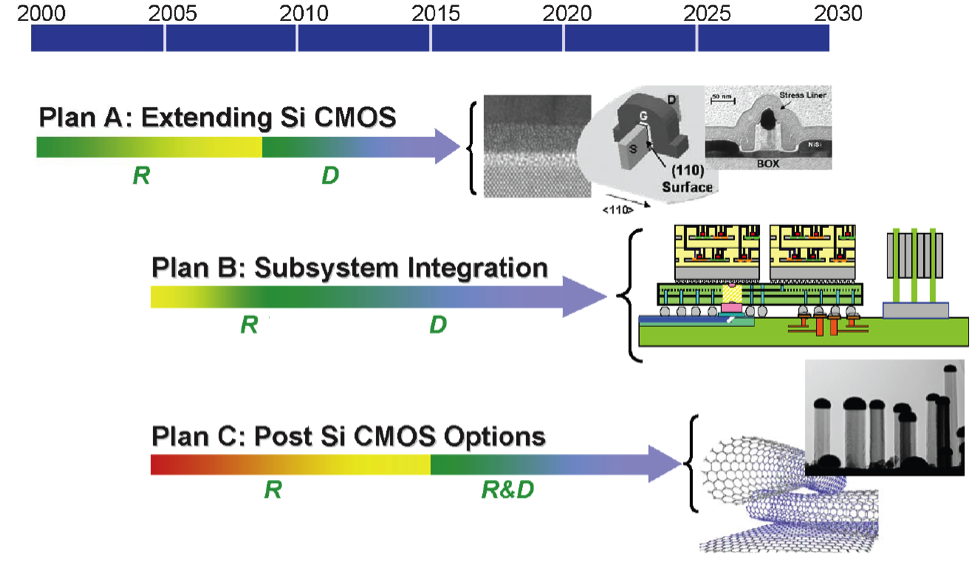
| Lecture 12 Strained Si technology and channel orientation | “Grand challenges” listed in ITRS, strained-Si technology, channel orientation |
| Lecture 13 Gate oxide and high-k | Reliability of thin SiO2, oxide breakdown, high-k dielectrics, metal gates |
| Lecture 14 Process-induced variability | Random dopant fluctuations, line edge roughness, metal grain granularity; associated variations in Vt and GIDL |
| Lecture 15 Interface effects | Band bending at the interface, interface and surface states, quantum effects in inversion layer |
| Lecture 16 Heterostructures and quantum confinement effects | Resonant tunneling devices (Shur 2.12), 3D, 2D, 1D structures, nanofabrication (reading) |
| Lecture 17 HEMT devices | Modulation doping, HEMT, |
| Lecture 18 Device Simulation | Partial differential equation solutions, Monte Carlo, Using Synopsis Sentaurus on CAEN |
| Lecture 19 Boltzmann Transport Equation | Boltzmann transport equation, approximations, applications and limitations |
| Lecture 20 Single electron devices | Coulomb blockade phenomena, Single electron transistors (Waser 16) |
| Lecture 21 Ballistic transistors | Ballistic transport, quantum “contact” resistance, properties of ballistic FET (notes) |
| Lectures 22 Graphene and other 2D material devices | Band structure (gapless semiconductor), transport properties and devices (Waser 9, notes) |
| Lecture 23 Memories 1 | DRAM and scaling, Flash memory and scaling, 3D flash |
| Lecture 24 Emerging memory and architectures | Resistive memory and STT MRAM. Emerging memory and logic architectures (Waser 22, 23, 28, notes) |
| Lecture 25 BEOL and 3D integration | BEOL processes, TSV, chip-on-wafer, monolithic BEOL integration |