MENU
MENU 

EECS 423: Micro/Nano Device Fabrication and Characterization
Instructor: Professor Jerzy Kanicki
Coverage
Learn basic principles and have hands-on experience with semiconductor fabrication technologies and device testing. Each student will fabricate and test polycrystalline Si gate, n-channel enhancement Si Metal Oxide Semiconductor Field Effect Transistors (MOSFETs) and related devices throughout the course. Fabrication technology including lithography, etching, deposition, oxidation, diffusion, and annealing will be studied. Students will practice the semiconductor fabrication technology in the cleanroom of the Lurie Nanofabrication Facility.
Lab
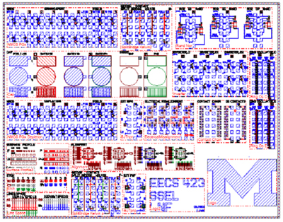
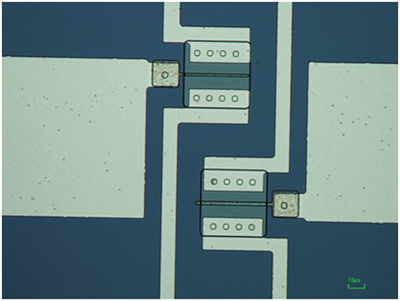
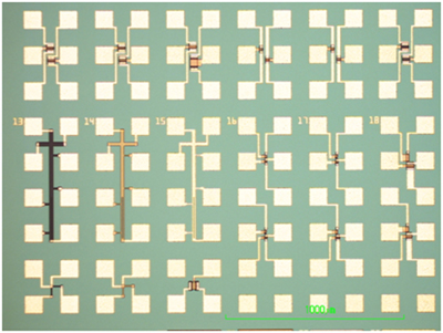
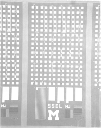
In the cleanroom of the Lurie Nanofabrication Facility, transistors, capacitors, and diodes with various designs will be fabricated on Si wafers. After completion of the fabrication, the electrical performance of these devices will be characterized in the testing lab.
Textbook(s)
Campbell, Stephen A. Fabrication Engineering at the Micro and Nanoscale (The Oxford Series in Electrical and Computer Engineering). 3 ed. New York: Oxford University Press, USA, 2007.
Syllabus
- Cleanroom Orientation
- Semiconductor crystal and wafers
- Oxidation
- Lithography
- Deposition
- Diffusion and doping
- Etching
- Thermal Annealing
- Contacts and interconnects
- Challenges and future trends of semiconductor technology