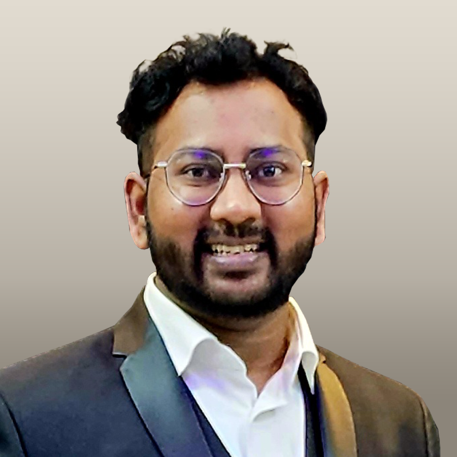
Faculty Candidate Seminar
Engineering Ultrawide Bandgap Semiconductors at the Atomic Scale
This event is free and open to the publicAdd to Google Calendar

Abstract: At the heart of rapidly evolving electronic devices is a meticulously engineered semiconductor material system. Atomic-level defects play a fundamental role in controlling the properties of semiconductors. Often, the level at which these defects need to be engineered can be as small as parts per billion. My research grapples with this formidable challenge by drawing on tools and concepts from thermodynamics and kinetics to develop predictive frameworks for systematic defect management, thereby enabling pathways for cutting-edge technologies. With the ubiquitous demand for higher-power electronics, shorter wavelength optoelectronics, and faster computing than what the incumbent technologies offer my research aims to implement ultrawide (>4.5 eV) bandgap (UWBG) semiconductors for developing next-generation electronic devices. The success of these new-generation semiconductor technologies hinges on the ability to overcome several, unique material and device challenges that become more pronounced as the bandgap increases. In this seminar, I will discuss how my research addresses this conundrum by encompassing several domains ranging from epitaxial growth, design, fabrication, and characterization of these devices with an emphasis on point defect management, structure-property correlations, and carrier transport physics. I will share several examples where such an approach to integrate materials science, physics, and electrical engineering allowed us to demonstrate cutting-edge devices while also striving toward boosting the performance to the theoretical limit, thus unlocking the consummate potential of UWBG semiconductors to enable disruptive technological changes.
Bio: Shashwat Rathkanthiwar is the Director of MOCVD Research at Lit Thinking Ultrawide Bandgap Semiconductor Research Center based in Orlando, Florida. Shashwat earned his undergraduate degree in Metallurgical and Materials Engineering shifting gears to Nano Science and Engineering for his doctorate at the Indian Institute of Science where his thesis focused on III-nitride ultraviolet optoelectronics. His postdoctoral tenure at North Carolina State University’s WideBandgaps Laboratory honed his expertise in epitaxially grown III-nitride semiconductors on native substrates, addressing doping, point defect management, and strain relaxation. His research integrates semiconductor materials science, physics, and electronics, envisioning revolutionary advancements in electronic, optical, quantum, and critical device technologies.
 MENU
MENU 
