ECE Distinguished Seminar Series
Electronics on anything – how thin film electronics can instrument the world
This event is free and open to the publicAdd to Google Calendar

Silicon electronics have revolutionized the processing and handling of information. The high temperatures required to create crystalline silicon devices, however, has limited the application of crystalline silicon to sensing systems that work in a small and mechanically rigid form factor. The development of inorganic and organic thin film electronics has launched a second revolution in electronics, granting the ability to process electronically active materials at low temperatures. This has allowed for two exciting opportunities: the ability to build electronic devices on the same size scale as the systems they interact with, and the ability to integrate electronic materials on a range of substrates including the back-end of CMOS integrated circuits, electronically active substrates, and flexible materials.
Our group has been working on the hybrid integration of organic semiconductors, thin film piezoelectrics, and laser-recrystallized silicon with active substrates to implement a range of new functionalities. In this presentation, I’ll show how thin film electronics and the hybrid integration enabled by new semiconductor systems and process options allows for active and spatially localized control of systems that are typically used in a single element format. Devices we have developed include single chip PCR systems, miniature spectrometers, devices for blood flow analysis, large area and miniature microphones, integrated on-chip filters, and active matrix micro-LED displays. These approaches unlock new applications in healthcare, sensing, displays, and communications.
Bio:
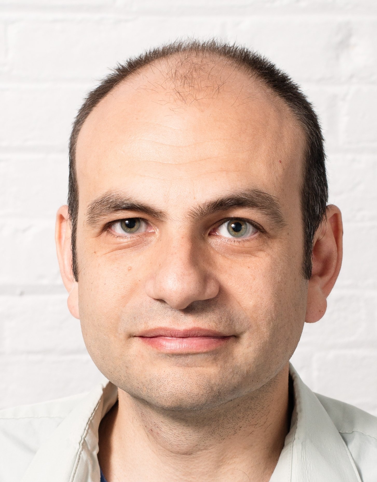
Ioannis (John) Kymissis is the Kenneth Brayer Professor of Electrical Engineering at Columbia University and Chair of the Department of Electrical Engineering. He graduated with his SB, M.Eng., and Ph.D. degrees from MIT. His M.Eng. thesis was performed as a co-op at the IBM T.J. Watson Research Lab on organic thin-film transistors, and his Ph.D. was obtained in the Microsystems Technology Lab at MIT, working on field-emission displays. After graduation, he spent three years as a postdoc in MIT’s Laboratory for Organic Optics and Electronics, working on a variety of organic electronic devices, and also as a senior engineer for QD Vision (later acquired by Samsung Electronics). He joined the faculty at Columbia University in electrical engineering as an assistant professor in 2006. He is a fellow of the IEEE, Optica, and the Society for Information Display (SID), and is currently the president-elect for SID.
 MENU
MENU 
