MIPSE Seminar
Rethinking the Art of Plasma Etch
This event is free and open to the publicAdd to Google Calendar

The seminar is free and open to the public. To request the Zoom link, please send an email to:
[email protected].
Abstract:
Since the 1970s, the semiconductor industry has fabricated electronic circuits using a plasma based pattern-transfer approach that is remarkably reminiscent of the etching artform used centuries ago. Only now, the patterns are a million times smaller and driven by the wafer fab equipment industry. The most advanced plasma etching technique in production today is called atomic layer etching (ALE) in which a single layer is re-moved in a cyclic manner. This talk will review the ALE approach in comparison to conventional plasma etching techniques, such as Reactive Ion Etching (RIE). As RIE reaches its fifth decade, its drawbacks have become apparent. ALE offers better control by isolating steps in time and switching between the steps in a repeatable cycle. To the extent that an ALE process behaves ideally – with high ALE synergy and self-limiting behavior – the primary benefit is improved uniformity across all length scales: at the surface, between different aspect ratios, and across the full wafer. Another benefit that will be highlighted is the atomic-scale smoothness in topography of the surface left behind after etching. The underlying mechanism and benefits of plasma ALE will be described, providing insight into the plasma science be-hind the ancient art of etching. Overall, ALE is simpler to under-stand than conventional plasma etch processing, and is proving to be important as we apply the art of etch at the atomic scale.
About the Speaker:
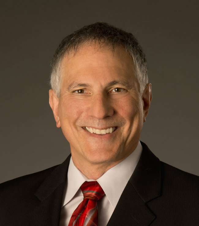
Richard A. Gottscho is Executive VP, Chief Technology Officer at Lam Research since May 2017. He previously was Executive VP, Global Products Group beginning August 2010; and group VP and general manager, Etch Businesses beginning March 2007. He joined Lam in January 1996 and has held various director and VP roles spanning deposition, etch, and clean products. Prior to joining Lam, he was at Bell Laboratories for 15 years, where he headed research departments in electronics materials, electronics packaging, and flat panel displays. In 2016, Dr. Gottscho was elected to the National Academy of Engineering. He has received several awards, including the AVS Peter Mark Memorial Award, AVS Plasma Science and Technology Division Prize, the Dry Process Symposium Nishizawa Award, and the Tegal Thinker Award. He is a fellow of the APS and AVS. He has authored numerous papers, patents, and lectures, and has served on journal editorial boards and program committees for major conferences in plasma science and engineering. He served as vice-chair of a National Research Council study on plasma science. Dr. Gottscho earned Ph.D. and B.S. degrees in physical chemistry from the Massachusetts Institute of Technology and Pennsylvania State University, respectively.
 MENU
MENU 
