 MENU
MENU 

ECE Seminar
Fabrication of advanced 2D and 3D nano-devices using NanoFrazor lithography
Thermal scanning probe lithography (t-SPL) has recently entered the lithography market as first true alternative or extension to electron beam lithography (EBL). The first dedicated t-SPL systems, called NanoFrazor, have been installed at research facilities in Europe, America, Asia and Australia by the company SwissLitho, a spinoff company of ETH Zurich.
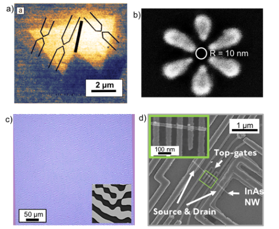
Core of the technology – which has its origins at IBM Research and their Millipede project – is a heatable ultra-sharp probe tip which is used for patterning and simultaneous inspection of complex nanostructures. The heated tip creates arbitrary depth, high-resolution (<10 nm half-pitch) nanostructures by local evaporation of resist materials. Using an integrated in-situ metrology method, the patterning depth can be controlled with 1 nm accuracy. This enables patterning of extremely accurate 3D nanostructures in a single step without wet development. The patterning speed is comparable to high resolution EBL. The application range for this new nanofabrication capability is broad and will be demonstrated with the discussion of a selection of examples.
Applications that are enabled by the nm-precise 3D patterning include 3D phase plates and finely tuned coupled Gaussian optical microcavities. Furthermore, 3D shaped nanofluidic confinements have been used to precisely control the movement of nanoparticles and nanowires. The high resolution 2D capability was applied e.g. to shape complex plasmonic structures. Furthermore, several superior nanoelectronic devices will be shown. Such devices are predominantly made from randomly dispersed nanowires or 2D materials. Therefore, they benefit strongly from the unique markerless overlay capability of the NanoFrazor lithography, but also from the fact that actually no charged particle beam is used during lithography, which can often damage sensitive materials. Finally, a few examples are shown, how the heated tips are also used for direct modification of surfaces by triggering of a local phase change or a chemical reaction.
Emine Cagin leads the Process and Applications Laboratory at SwissLitho AG. She received her MSc and PhD degrees in electrical engineering from the University of Michigan in Ann Arbor, where she studied the interfaces of ferroelectric materials with semiconducting ZnO. She then did a post-doctoral fellowship at ETH Zürich in the Micro and Nanosystems group, focusing on electrical contacts to carbon nanotubes. Prior to joining SwissLitho, she was a senior staff scientist at NTB Buchs, where she led applied research projects in microtechnology in close collaboration with industry partners.